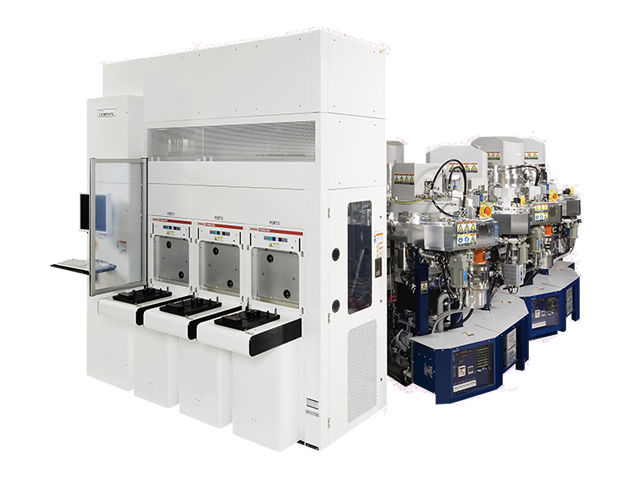
Key Features
- Flexible module configuration.
- The integration of PVD and CVD/ALD process.
- The various applications (NVM, Al & Cu wiring, TI/TiN barrier metal, thick AL and Co/Ni salicide etc.).
- Process capability for not only Si devices but also compound semiconductor, on quartz devices, etc.
- 10 process modules maximum can be equipped based on the cluster tool concept.
- Single or Tandem platform is available.
- Wafer transfer speed is 60% up. High reductivity and low CO2 were achieved.
- Environmental consideration Various energy saving functions were standard installed, and the energy saving of 30% on the current model was achieved.
- Equipped with the control system that comphes with the next generation semiconductor Fab. The excellent thin film contorol and EES compliance. The high advanced automation Fab compliance.
Need more information?
At ULVAC, we understand that finding the right product is crucial for optimizing your processes, whether you're scaling up production or maintaining precision in your systems. With our wide range of cutting-edge vacuum technologies and in-depth expertise, we will guide you through selecting the ideal solution tailored to your unique requirements.
Contact ULVAC System Sales & Support For inquiries outside North and South America, please contact ULVAC Corporate