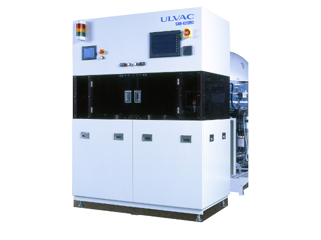
Features
- Applicable substrate size: φ125 to 200mm.
- Capable of auto-transfer for Ultra-thin Si wafer up to 50μm thickness.
- Up to 5 unique process recipes.
- Sputter-Etching process developed by ISM.
- Efficient water cooling mechanism by ESC method is available.
Applications
- Power device
- WL-CSP (seed layer of electrolytic plating)
- UBM (Barrier metal)
Need more information?
At ULVAC, we understand that finding the right product is crucial for optimizing your processes, whether you're scaling up production or maintaining precision in your systems. With our wide range of cutting-edge vacuum technologies and in-depth expertise, we will guide you through selecting the ideal solution tailored to your unique requirements.
Contact ULVAC System Sales & Support For inquiries outside North and South America, please contact ULVAC Corporate

